The semiconductor industry has surpassed the traditional steel industry and automobile industry and become a high value-added and high-tech industry in the 21st century. Semiconductors are the core of many industrial equipment, which are widely used in the core fields of computers, consumer electronics, network communications, automotive electronics and so on.
Semiconductors are mainly composed of four parts: integrated circuits, optoelectronic equipment, discrete equipment and sensors; Integrated circuit is the core of semiconductor industry, accounting for more than 80%. Integrated circuits include logic chips, memory chips, analog chips and MPUs. The rapid development of integrated circuits in performance, integration and speed is based on the development of semiconductor physics, semiconductor devices and semiconductor manufacturing technology.
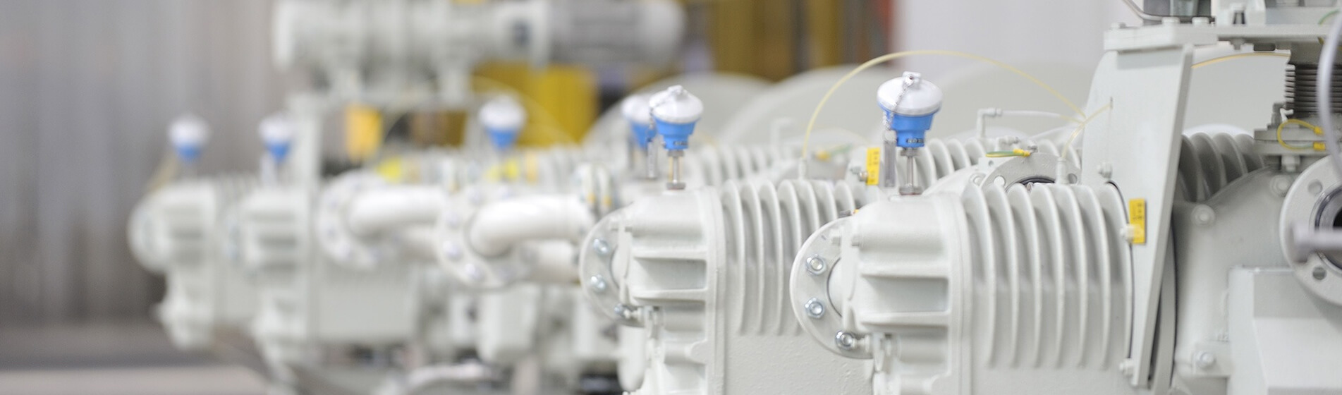
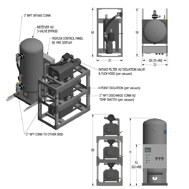
With such a huge market in the semiconductor industry, semiconductor process equipment provides a manufacturing foundation for large-scale semiconductor manufacturing. In the future, the integration and miniaturization of semiconductor devices will be higher and more powerful. The main equipment in the semiconductor production process is attached below.
1.Monocrystal furnace
Equipment function: melt semiconductor materials, pull single crystals, and provide single crystal semiconductor billets for subsequent semiconductor device manufacturing.

2.Gas phase epitaxial furnace
Equipment function: provide a specific process environment for gas phase epitaxy growth, realize the growth of thin-layer crystals corresponding to the monocrystalline phase on single crystals, and make basic preparations for the bottom sinking of single products to realize functionalization. Vapor phase epitaxy is a special process of chemical vapor deposition. The body structure of the growth thin layer is the continuation of the single crystal substrate, and maintains a corresponding relationship with the crystal direction at the bottom of the village.

3.MBE system
Equipment function: molecular beam epitaxy system, providing process equipment for growing thin films on the bottom surface according to specific requirements; Molecular beam epitaxy is a technology for preparing single crystal thin films. It is to grow thin films layer by layer along the crystal axis of the substrate material under appropriate substrates and conditions.

4.Oxidation furnace (VDF)
Equipment function: it is an indispensable part of semiconductor processing process to carry out oxidation treatment for semiconductor materials, provide the required oxidation atmosphere, and realize the oxidation treatment process of semiconductor expected design.
")
5.Low pressure chemical vapor deposition system (LPCVD)
Equipment function: introduce the vapor containing gaseous or liquid reactants constituting film elements and other gases required for the reaction into the reaction chamber of LPCVD equipment, and produce a film by chemical reaction on the surface of the substrate.
")
6.Plasma enhanced chemical vapor deposition system (PECVD)
Equipment function: use glow discharge in the deposition chamber to ionize it and then carry out chemical reaction on the substrate to deposit semiconductor thin film materials.
")
7.Magnetron sputtering station (MSA)
Equipment function: through a closed magnetic field parallel to the target surface in the two pole splash and the orthogonal electromagnetic field formed on the target surface, the secondary electrons are bound to the specific area of the target surface to realize high ion density and high-energy ionization, and the target atoms or molecules are sputtered and deposited on the substrate at a high rate to form a thin film.
")
8.Chemical mechanical polishing machine (CMP)
Equipment function: grind and polish the ground body (semiconductor) through the combined action of mechanical grinding and chemical liquid dissolution "corrosion".
")
9.Lithography machine
Equipment function: evenly glue the surface of semiconductor substrate (silicon wafer), transfer the graphics on the mask to the photoresist, and temporarily "copy" the device or circuit structure to the silicon wafer.

10.Reactive ion etching system (RIE)
Equipment function: apply high-frequency voltage between plate electrodes to produce hundreds of microns thick ion layer, put in the pattern, and the pattern of high-speed impact of ions, so as to realize chemical reaction etching and physical impact, and realize the processing and molding of semiconductors.
")
11.ICP plasma etching system
Equipment function: one or more gas atoms or molecules are mixed in the reaction chamber to form a plasma under the action of external energy (such as RF, microwave, etc.). On the one hand, the active groups in the plasma react with the surface materials to be etched to produce volatile products; on the other hand, the ions in the plasma are guided and accelerated under the action of bias voltage to realize directional corrosion and accelerated corrosion of the surface to be etched.

12.Wet etching and cleaning machine
Equipment function: wet etching is the technology of immersing etching materials in corrosive solution for corrosion. Cleaning is to reduce contamination, which will affect the performance of devices, cause reliability problems and reduce the yield, which requires thorough cleaning before the next process of each layer or before the next layer

13.Ion implanter (IBI)
Equipment function: doping the area near the semiconductor surface.
")
14.Probe test bench
Equipment function: through the contact between the probe and the pad of semiconductor devices, electrical tests are carried out to detect whether the performance indicators of semiconductors meet the design performance requirements.

15.Wafer thinning machine
Equipment function: reduce the thickness of wafer by polishing

16.Wafer dicing machine (DS)
Device function: cut the wafer into small pieces of die.
")
17.Wire bonder
Device function: connect the pad on the semiconductor chip and the pad on the pin with conductive metal wire (gold wire).

Tel : +86-15880223078
WhatsApp : +86-13959235484
Email : vacuum@xiamenbest.com
Address : No. 19, Dongan Qianzhanli, Jimei District, Xiamen city china